Can Microvia Be Used
In today’s increasingly high-performance, compact electronic devices, microvias are a vital technology for connecting circuit boards and enabling greater functionality. These miniature vias, fabricated layer by layer, save space and can also improve PCB manufacturing efficiency. Nevertheless, there are some reliability concerns that must be addressed in order to ensure that the microvia-based interconnects can perform in harsh environments.
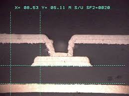
These metallization issues can be caused by the coefficient of thermal expansion (CTE) mismatch between a microvia structure’s copper plating and the dielectric materials surrounding it. The mismatch creates stresses that can lead to failure at the plated interfaces, particularly at the microvia/via or via/pad connections. Various types of failures, including interfacial separation (between the base of the via and the taget pad) barrel cracks (around the head of the via), and corner/knee cracks, can also occur.
The underlying issue that leads to these problems is the use of a low-cost copper alloy for plating the microvia. This alloy has a significantly higher CTE than the pure copper used in conventional plating processes, and this difference creates stress concentrations along the walls of the via. These stress concentrations can cause premature cracking during reflow or during operation of the device.
Can Microvia Be Used in Harsh Environments?
In order to improve these issues, many PCB manufacturers are moving towards the use of conductive inks and pastes for filling the microvias instead of traditional copper plating. This provides a better electrical performance and reduced voiding, as well as improved thermal conductivity. This can help to reduce the risks associated with using a plated-over-copper process, and these inks and pastes are also easier to handle than standard copper plating.
Another improvement that is being made with microvias is their ability to be drilled, filled, and plated without the need for mechanical drilling equipment. This is a significant advancement because mechanically-drilled holes can be susceptible to vibration and fatigue, leading to failures during the fabrication process. Laser-drilled microvias, on the other hand, can be drilled much smaller than traditional through-hole vias and are more reliable during manufacturing.
To create a PCB with microvias, it is important to start by designing the padstack in Padstack Editor. Once the padstack is defined, you can then add the microvia layers to the stackup and define the dimensions. Finally, you will need to select an appropriate laminate to ensure that the microvias can be fabricated. If you are unsure of which laminate to choose, I recommend that you consult with your fabricator and ask for their input. This will help you to make the best decisions for your project and ensure that your microvias will be manufacturable. Then you can begin to build your prototype.