
PCB Fabrication Assembly
When electric current flows through a circuit board, it creates an electromagnetic field that radiates outward. This energy can disturb other electronic devices operating in close proximity, resulting in a disturbance called electromagnetic interference (EMI). PCB designers must follow good practices that aim to curb EMI and maintain a high level of electromagnetic compatibility or EMC.
EMI is often caused by long traces that act as transmission lines. These can leak electromagnetic fields into other traces on the same board or other boards in the system, creating crosstalk and other problems. This is why it’s important to keep traces as short as possible.
Other common EMI issues arise due to component inefficiency or malfunction. For example, if power and ground lines are not decoupled, they can cause voltage fluctuations that lead to instability or failure. It’s important to minimize EMI by implementing proper design and assembly techniques.
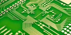
How PCB Fabrication Assembly Handles Electromagnetic Interference
To prevent EMI, a number of steps are typically taken during pcb fabrication assembly. Some of these include shielding and encapsulation. Shielding involves adding a metal enclosure around sensitive areas of the board to block EMI from entering or leaving it. In addition, conductive coatings can be applied to critical areas of the board to trap and dissipate interference.
Other EMI reduction methods include decoupling power and ground lines and adding capacitive filters to signal pairs. These filters help to shunt EMI to ground, allowing the high-frequency signals to reach their destinations without being disturbed. Ferrite beads or chips are also commonly used to absorb and dissipate high-frequency interference.
Another way to reduce EMI is to use a copper or aluminum conductive coating to shield critical areas of the circuit board. These coatings are usually deposited as an adhesive-backed tape on the top and bottom of the board, forming an electrically continuous shield to prevent interference from penetrating the circuit. Conductive gaskets and seals are also sometimes used to close gaps between the PCB and its enclosure, preventing EMI from escaping.
Once the PCB has been fabricated, it’s ready for final assembly and testing. During this step, the boards are removed from their manufacturing panels and placed on a testing fixture for continuity testing with a bed of nails test fixture or flying probe test system. During this process, the continuity tester looks for any unintentional shorts between nets that could cause malfunction or failure.
In addition to reducing EMI, these tests can also help to find any other flaws in the design. These flaws may be minor, but can still cause performance or reliability issues in the end product. For example, a defect in the PCB’s ground plane can result in a voltage drop that causes signal timing errors during data transfer. Luckily, this problem can be avoided by routing the traces to a single large ground plane during PCB layout.