
Flex Circuit PCBs
The leading conductor material for flex circuit PCBs is copper foil, but other metals such as aluminum and nickel are also used. These materials are usually rolled and annealed to improve their flexibility. The most commonly used insulator is polyimide, but FR4 and glass fiber matts are also used. In a multi-layered flex PCB, polyimide is typically used as the dielectric insulator and coverlay layer. Its film structure makes it more flexible than FR-4, and its lower dielectric constant (Dk) helps achieve controlled impedance for higher speed applications.
A flex circuit is a multi-layer printed circuit board that can be bent and folded without breaking or destroying the internal wiring. The layers of a flex PCB are bonded together using acrylic thermally-cured adhesives. A flex PCB is a complex structure with multiple conductive paths, holes, and connectors. In order to prevent these traces from damaging each other, the PCB must be stiffened in some areas by attaching rigid components known as stiffeners to it. Stiffeners are often made of a non-conductive material such as FR4 or Kapton. They are attached to the flex circuit using acrylic or epoxy adhesives, and they provide structural reinforcement for the flex. They can also be used to reduce bending stresses, add weight balance, and dissipate heat.
As a result of the unique manufacturing and assembly process, flex circuit pcb must adhere to special requirements to ensure dependable operation. The most important requirement is the control of impedance, which must be achieved in the flex stack-up to minimize signal reflections and achieve consistent performance. To ensure a successful flex circuit, it is crucial to follow IPC-610 and consult your CM’s engineering team for expert advice on your design.
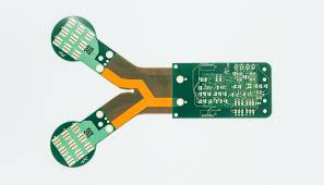
Materials Used in Flex Circuit PCBs
Using the right materials and design rules is critical for the success of any flex circuit project. Narrower traces require increased flex spacing to avoid cracks, and a 2:1 ratio of spacing to trace width is recommended. Additionally, a high-speed flex PCB requires low DK and thinner copper thickness to enable it to operate at high frequencies.
In a flex PCB, plated through-holes (vias) are connected to the copper traces using either teardrop or annular rings. Teardrop-shaped vias are more suitable for flex applications because they allow a larger connection area and less stress concentration. Annular rings are also a good choice for flex circuits, but they must be smaller to accommodate the increased movement and contraction of the flex material.
After the flex PCB is assembled, it undergoes a baking process to remove any moisture and to prepare it for solder paste printing. The metallization is then applied to the copper traces and through-holes, and solder is deposited through the holes using a stencil and a tool called a squeegee. In addition, a hot-melt adhesive or a silicone is used to attach the components to the stiffeners and flex material. Finally, the flex PCB undergoes a test to verify its reliability. This includes measuring the flex circuit’s maximum load-carrying capabilities, minimum bend radius, and impedance.