
Wave Soldering for SMT Circuit Board
As printed circuit boards (PCBs) grew more complex, through-hole assemblies gave way to “hybrid” assemblies that combined through-hole and surface-mount devices. These new types of PCBs introduced a whole host of issues, from incomplete solder fillets to bridging to resin smear on the pads and other surfaces. Some of these new issues were solved by adding glue and using heated rollers to melt it onto the board, but this added cost and required additional equipment for maintenance and operation. Other issues required the use of higher temperatures, and that meant adding even more energy to the process.
Solder bridging occurs when the metallization on the top of the component leads makes contact with the plated copper on the bottom of the component. This often results in short circuits. Incomplete solder fillets can be caused by the hole-to-lead ratio, steep conveyor angles, excessive wave temperature or contamination on the edge of the pads from burring, drilling or punching during manufacturing. Other causes include poor board alignment or the fact that some areas of the board are not exposed to the wave, as illustrated in Figure 1.
There are many ways to prevent bridging on your smt circuit board, but most of them focus on the front end of the process: getting the flux down, getting the lead lengths cut, doing everything you can on the assembly side of the process to ensure good adhesion. However, no matter how well you manage those factors, bridging will still occur – it’s just the nature of fluid dynamics in the soldering process.
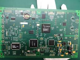
Optimize Conveyor Angle in Wave Soldering for SMT Circuit Board
Fortunately, we have evolved through several generations of wave soldering machines with engineering genius that has addressed these problems. The basic design is that the conveyor and wave are set up so that all of the solder flow over the front baffle. As the assembly enters the wave, it pushes the solder back over the front baffle and some of it moves over the rear one. Because of surface tension, the majority of the solder plows into and contacts the through-hole leads if the assembly is properly aligned. However, if the assembly is not aligned properly, some of the solder forms an elastic membrane that stretches like a solid web or taffy pull as it moves farther from the wave. The membrane can snap to the leads and cause a bridge.
The solution is to tilt the conveyor chain by a small amount and provide a conveyor angle that allows some of that excess molten solder to flow back into the machine via gravity. It also provides a little more time for the solder to be deposited on the leads, reducing the chance of bridging.
The problem is that you need to do this for every single conveyor and wave on your line, and the variation in the variables can be considerable. This is where a slew of optimization methods have come into play, including Taguchi method, neural networks and fractional factorial design. These methods identify the dominant process parameters that impact your smt circuit board soldering and can predict the optimum control points to improve quality, reliability and productivity.